Zynq-7000 AP SoC and 7 Series FPGAs MIS v4.1 347
UG586 November 30, 2016
www.xilinx.com
Chapter 2: QDR II+ Memory Interface Solution
For QDR II+ SRAM interfaces that have the memory system input clock
(sys_clk_p/sys_clk_n) placed on CCIO pins within one of the memory banks, MIG
assigns the DIFF_HSTL_I I/O standard (VCCO = 1.5V) to the CCIO pins. Because the same
differential input receiver is used for both DIFF_HSTL_I and LVDS inputs, an LVDS clock
source can be connected directly to the DIFF_HSTL_I CCIO pins. For more details on usage
and required circuitry for LVDS and LVDS_25 I/O Standards, see the 7Series FPGAs
SelectIO™ Resources User Guide (UG471) [Ref 2].
Termination
These recommendations apply to termination for QDR II+ SRAM:
• Simulation (using IBIS or other) is highly recommended. The loading of command and
address signals depends on various factors, such as speed requirements and
termination topology. Loading can be a limiting factor in reaching a performance
target.
• Command and Address signals should be terminated to V
TT
through a 50Ω resistor.
• Write Clock (K_P/N) does not require an external termination if ODT is available. If ODT
is not available, each line should be terminated to V
TT
through a 50Ω resistor.
• Write Data lines (D) do not require an external termination if ODT is available. If ODT is
not available, each line should be terminated to V
TT
through a 50Ω resistor.
• Read Clock (CQ) does not require an external termination and should use DCI. Set the
DCI termination for each single-ended line to 50Ω.
• Read Data lines (Q, QVLD) do not require an external termination and should use DCI.
Set the DCI termination to 50Ω.
I/O Standards
The MIG tool generates the appropriate XDC for the core with SelectIO™ interface
standards based on the type of input or output to the 7 series FPGAs. These standards
should not be changed. Table 2-14 contains a list of the ports together with the I/O
standard used.
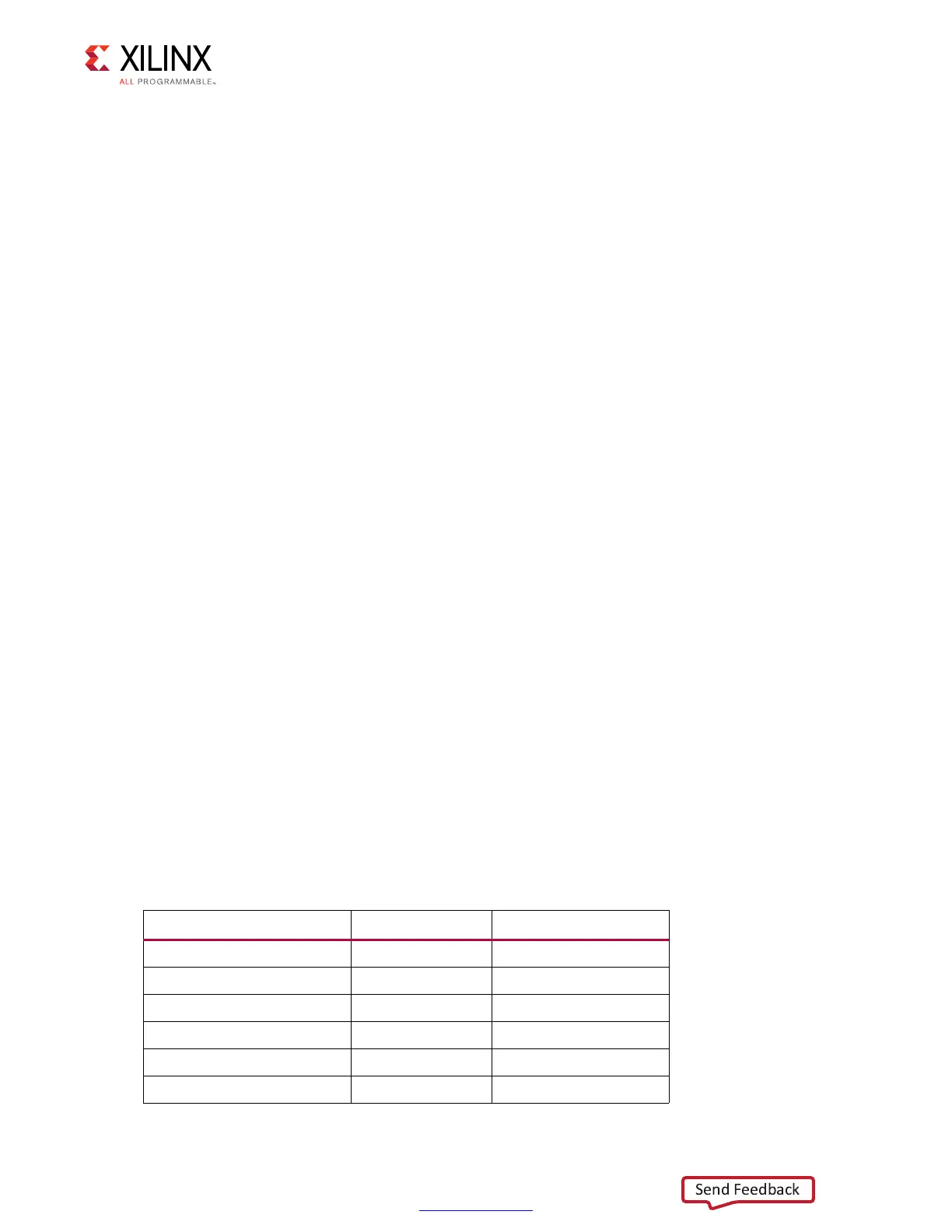
Table 2-14: I/O Standards
Signal
(1)
Direction I/O Standard
qdr_bw_n Output HSTL_I
qdr_cq_p, qdr_cq_n Input HSTL_I_DCI
qdr_d Output HSTL_I
qdr_k_p, qdr_k_n InOut DIFF_HSTL_II
qdr_q Input HSTL_I_DCI
qdr_r_n Output HSTL_I