Zynq-7000 AP SoC and 7 Series FPGAs MIS v4.1 120
UG586 November 30, 2016
www.xilinx.com
Chapter 1: DDR3 and DDR2 SDRAM Memory Interface Solution
• When HR banks are selected for memory interface pins in GUI and the memory
frequencies ≥ 400 MHz, the phase is 337.5°.
• When HR banks are selected for memory interface pins in GUI and the memory
frequencies are between 200–400 MHz (excluding 400 MHz), the phase is 0°.
The default setting for the PLL multiply (M) and divide (D) values is for the system clock
input frequency to be equal to the memory clock frequency. This 1:1 ratio is not required.
The PLL input divider (D) can be any value listed in the 7 Series FPGAs Clocking Resources
User Guide (UG472) [Ref 10] as long as the PLLE2 operating conditions are met and the
other constraints listed here are observed. The PLL multiply (M) value must be between 1
and 16 inclusive. The PLL output divider (O) for the memory clock must be 2 for 800 Mb/s
and above, and 4 for 400 to 800 Mb/s. The PLL VCO frequency range must be kept in the
range specified in the silicon data sheet. The sync_pulse must be 1/16 of the mem_refclk
frequency and must have a duty cycle of 1/16 or 6.25%. For information on physical
placement of the PLL and the System Clock CCIO input, see Design Guidelines, page 192.
The details of the ISERDES/OSERDES connectivity are shown in Figure 1-58, page 141 and
Figure 1-60, page 143.
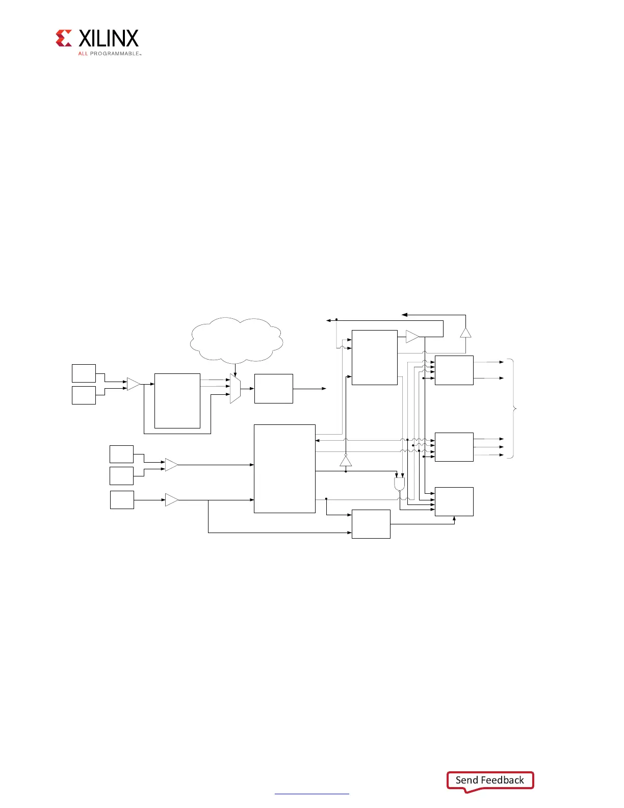
Internal (FPGA) Logic Clock
The internal FPGA logic is clocked by a global clocking resource at a half or quarter
frequency of the DDR2 or DDR3 SDRAM clock frequency, which depends on 4:1 or 2:1 mode
selected in the MIG tool. This PLL also outputs the high-speed DDR2 or DDR3 memory
clock.
X-Ref Target - Figure 1-52
Figure 1-52: Clocking Architecture
CLKREF
N
CLKREF
P
Phaser_IN
Phaser_OUT
PHY Control
0+],'(/$<
5HIHUHQFH&ORFN
)RU''5GHVLJQIUHTXHQFLHV!0+]
,'(/$<&75/FORFNRI0+]LV
VHOHFWHGEDVHGRQ)3*$GHYLFHVSHHGJUDGH
)RURWKHUV0+]FORFNLVVHOHFWHG
MMCM
&/.,1
&/.287
&/.287
0+]
0+]
0+]
IDELAYCTRL
LGHOD\FWUOBUG\
MMCM
&/.,1
&/.)%287
/2&.('
&/.)%,1
567
PHASER_REF
&/.,1
567
PLL
&/.,1
&/.287
&/.287567
&/.287
&/.287
/2&.('
SYSCKN
SYSCKP
6\VWHP&ORFN,QSXW3DLU
SYSRST
,%8)*'6
,%8)
UHIBGOOBORFN
2&/.
2&/.',9
2&/.B'(/$<('
,&/.
,&/.',9
,QWHUQDO)3*$/RJLF&ORFN
IUHTBUHIFON
3+<B&ON
%8)*
V\QFBSXOVH
PHPBUHIFON
SOOBORFN
,6(5'(626(5'(6
&RQQHFWLYLW\
%8)*
00&03KDVH6KLIW&ORFN
 Loading...


