Zynq-7000 AP SoC and 7 Series FPGAs MIS v4.1 458
UG586 November 30, 2016
www.xilinx.com
Chapter 3: RLDRAM II and RLDRAM 3 Memory Interface Solutions
Customizing the Core
The RLDRAM II/RLDRAM 3 memory interface solution is customizable to support several
configurations. The specific configuration is defined by Verilog parameters in the top-level
of the core. As per the OOC flow, none of the parameter values are passed down to the user
design RTL file from the example design top RTL file. So, any design related parameter
change is not reflected in the user design logic. The MIG tool should be used to regenerate
a design when parameters need to be changed. The parameters are summarized in
Table 3-14.
X-Ref Target - Figure 3-60
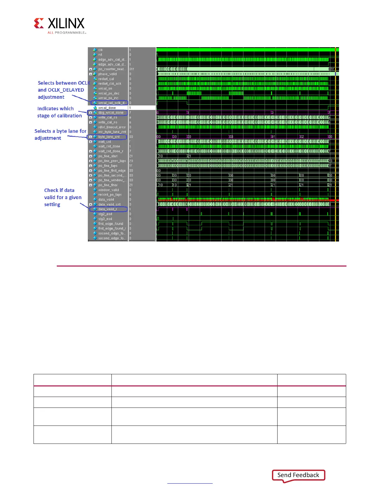
Figure 3-60: RLDRAM II Write Calibration Waveforms
Table 3-14: RLDRAM II Memory Interface Solution Configurable Parameters
Parameter Description Options
CLK_PERIOD Memory clock period (ps). –
ADDR_WIDTH Memory address bus width. 18–22
RLD_ADDR_WIDTH
Physical Memory address bus width when using Address
Multiplexing mode.
11, 18–22
BANK_WIDTH Memory bank address bus width.
RLDRAM II: 3
RLDRAM 3: 4
 Loading...


