Zynq-7000 AP SoC and 7 Series FPGAs MIS v4.1 377
UG586 November 30, 2016
www.xilinx.com
Chapter 2: QDR II+ Memory Interface Solution
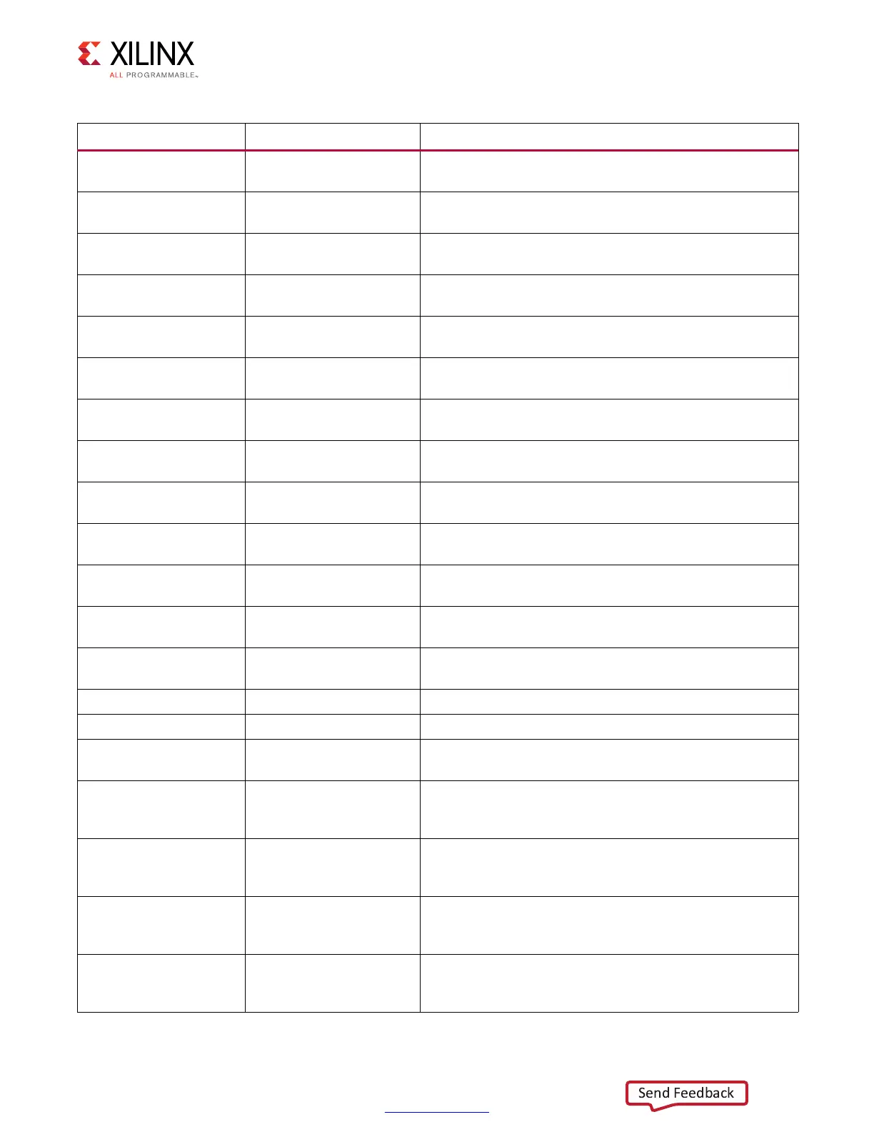
dbg_stage2_cal[10] edge_adv_cal_start
Indicates start of edge_adv calibration, to see if the
pi_edge_adv signal needs to be asserted
dbg_stage2_cal[11] rd0_vld
Indicates valid ISERDES read data for the byte being
calibrated (indicated by byte_cnt)
dbg_stage2_cal[12] fd0_vld
Indicates valid ISERDES read data for the byte being
calibrated (indicated by byte_cnt)
dbg_stage2_cal[13] rd1_vld
Indicates valid ISERDES read data for the byte being
calibrated (indicated by byte_cnt)
dbg_stage2_cal[14] fd1_vld
Indicates valid ISERDES read data for the byte being
calibrated (indicated by byte_cnt)
dbg_stage2_cal[15] phase_vld
Valid data is seen for the particular byte for the byte being
calibrated (indicated by byte_cnt)
dbg_stage2_cal[16] rd0_bslip_vld
Indicates valid ISERDES read data requiring bitslip for the
byte being calibrated (indicated by byte_cnt)
dbg_stage2_cal[17] fd0_bslip_vld
Indicates valid ISERDES read data requiring bitslip for the
byte being calibrated (indicated by byte_cnt)
dbg_stage2_cal[18] rd1_bslip_vld
Indicates valid ISERDES read data requiring bitslip for the
byte being calibrated (indicated by byte_cnt)
dbg_stage2_cal[19] fd1_bslip_vld
Indicates valid ISERDES read data requiring bitslip for the
byte being calibrated (indicated by byte_cnt)
dbg_stage2_cal[20] phase_bslip_vld
Valid data is seen when bitslip applied to read data for the
byte being calibrated (indicated by byte_cnt)
dbg_stage2_cal[21] clkdiv_phase_cal_done_4r
Indicates data validity complete, proceed to assert the
pi_edge_adv signal if needed
dbg_stage2_cal[22] pi_edge_adv
Phaser control signal to advance the Phaser clock, ICLKDIV
by one fast clk cycle. Only used for nCK_PER_CLK == 2.
dbg_stage2_cal[25:23] byte_cnt[2:0] Indicates the byte that is being checked for data validity
dbg_stage2_cal[26] inc_byte_cnt Internal signal to increment to the next byte
dbg_stage2_cal[29:27] pi_edge_adv_wait_cnt
Counter to wait between asserting the phaser control
signal, pi_edge_adv signal in the various byte lanes.
dbg_stage2_cal[30] bitslip
FPGA logic bitslip control signal, indicates when the logic
shifts the data alignment. Only used for nCK_PER_CLK ==
4.
dbg_stage2_cal[31] rd2_vld
Indicates valid ISERDES read data for the byte being
calibrated (indicated by byte_cnt). Only valid for
nCK_PER_CLK == 4.
dbg_stage2_cal[32] fd2_vld
Indicates valid ISERDES read data for the byte being
calibrated (indicated by byte_cnt). Only valid for
nCK_PER_CLK == 4.
dbg_stage2_cal[33] rd3_vld
Indicates valid ISERDES read data for the byte being
calibrated (indicated by byte_cnt). Only valid for
nCK_PER_CLK == 4.
Table 2-21: Read Stage 2 Debug Signal Map (Cont’d)
Bits PHY Signal Name Description
 Loading...


