Zynq-7000 AP SoC and 7 Series FPGAs MIS v4.1 99
UG586 November 30, 2016
www.xilinx.com
Chapter 1: DDR3 and DDR2 SDRAM Memory Interface Solution
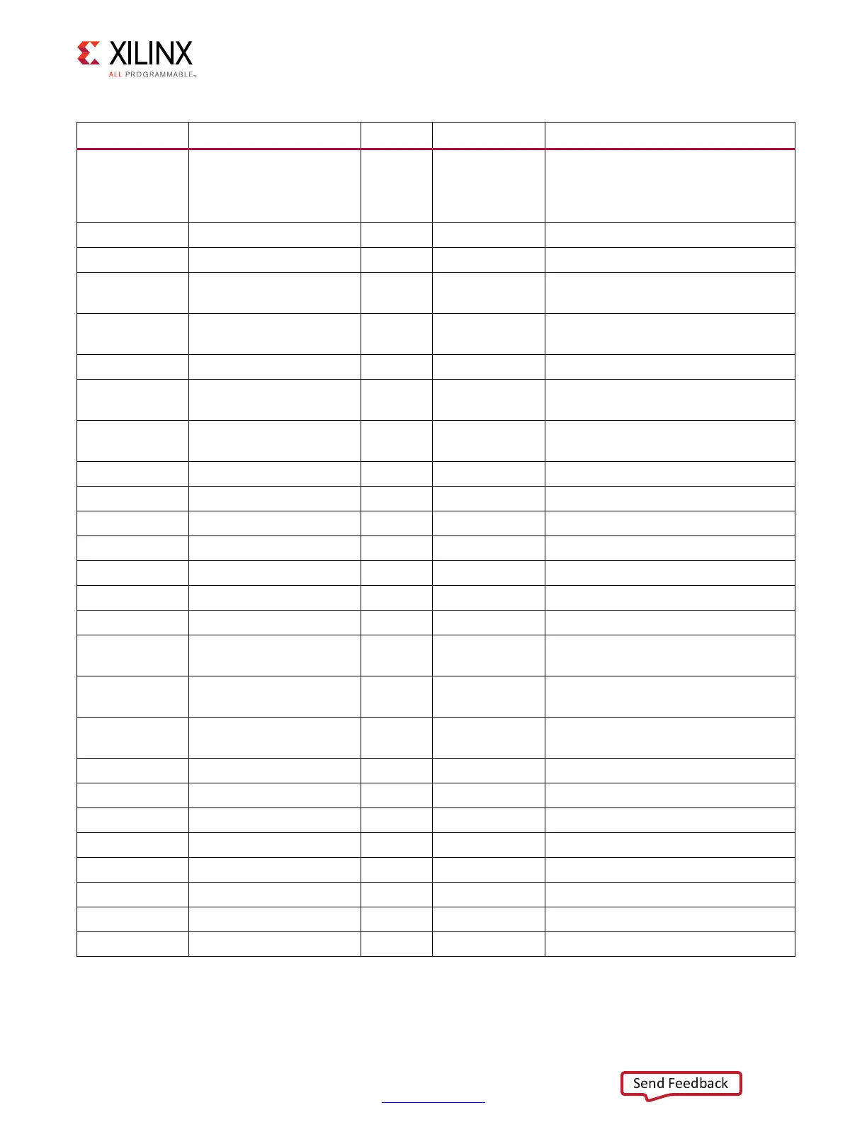
s_axi_awready 1 Output High
Write address ready. This signal
indicates that the slave is ready to
accept an address and associated
control signals.
s_axi_wdata C_AXI_DATA_WIDTH Input Write data.
s_axi_wstrb C_AXI_DATA_WIDTH/8 Input Write strobes.
s_axi_wlast 1 Input High
Write last. This signal indicates the
last transfer in a write burst.
s_axi_wvalid 1 Input High
Write valid. This signal indicates that
write data and strobe are available.
s_axi_wready 1 Output High Write ready.
s_axi_bid C_AXI_ID_WIDTH Output
Response ID. The identification tag of
the write response.
s_axi_bresp 2 Output
Write response. This signal indicates
the status of the write response.
s_axi_bvalid 1 Output High Write response valid.
s_axi_bready 1 Input High Response ready.
s_axi_arid C_AXI_ID_WIDTH Input Read address ID.
s_axi_araddr C_AXI_ADDR_WIDTH Input Read address.
s_axi_arlen 8 Input Read burst length.
s_axi_arsize 3 Input Read burst size.
s_axi_arburst 2 Input Read burst type.
s_axi_arlock 1 Input
Lock type. (This is not used in the
current implementation.)
s_axi_arcache 4 Input
Cache type. (This is not used in the
current implementation.)
s_axi_arprot 3 Input
Protection type. (This is not used in
the current implementation.)
s_axi_arvalid 1 Input High Read address valid.
s_axi_arready 1 Output High Read address ready.
s_axi_rid C_AXI_ID_WIDTH Output Read ID tag.
s_axi_rdata C_AXI_DATA_WIDTH Output Read data.
s_axi_rresp 2 Output Read response.
s_axi_rlast 1 Output Read last.
s_axi_rvalid 1 Output Read valid.
s_axi_rready 1 Input Read ready.
Table 1-20: AXI4 Slave Interface Signals (Cont’d)
Name Width Direction Active State Description
 Loading...


