Zynq-7000 AP SoC and 7 Series FPGAs MIS v4.1 167
UG586 November 30, 2016
www.xilinx.com
Chapter 1: DDR3 and DDR2 SDRAM Memory Interface Solution
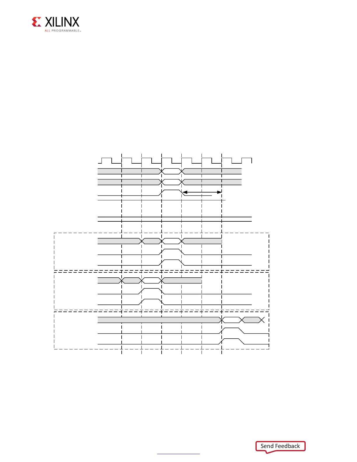
A non back-to-back write command can be issued as shown in Figure 1-75. This figure
depicts three scenarios for the app_wdf_data, app_wdf_wren, and app_wdf_end
signals, as follows:
1. Write data is presented along with the corresponding write command (second half of
BL8).
2. Write data is presented before the corresponding write command.
3. Write data is presented after the corresponding write command, but should not exceed
the limitation of two clock cycles.
For write data that is output after the write command has been registered, as shown in
Note 3, the maximum delay is two clock cycles.
X-Ref Target - Figure 1-75
Figure 1-75: 4:1 Mode UI Interface Write Timing Diagram (Memory Burst Type = BL8)
8*BFBB
DSSBZGIBGDWD
FON
DSSBFPG
:5,7(
DSSBDGGU
$GGU
DSSBZGIBHQG
DSSBHQ
DSSBZGIBZUHQ
DSSBUG\
DSSBZGIBPDVN
DSSBZGIBUG\
:
:
DSSBZGIBGDWD
DSSBZGIBHQG
DSSBZGIBZUHQ
DSSBZGIBGDWD
DSSBZGIBHQG
DSSBZGIBZUHQ
:
0D[LPXPDOORZHGGDWDGHOD\IURP
DGGUFPGLVWZRFORFNVDVVKRZQ
LQ(YHQW
 Loading...


