Zynq-7000 AP SoC and 7 Series FPGAs MIS v4.1 132
UG586 November 30, 2016
www.xilinx.com
Chapter 1: DDR3 and DDR2 SDRAM Memory Interface Solution
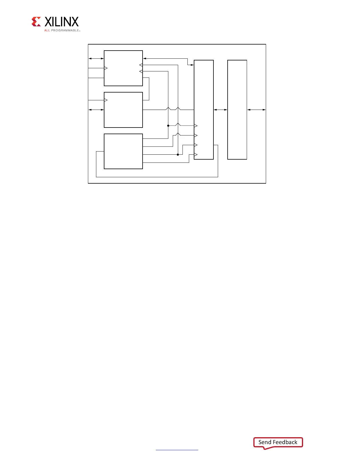
The Memory Controller and calibration logic communicate with this dedicated PHY in the
slow frequency clock domain, which is either a divided by 4 or divided by 2 version of the
DDR2 or DDR3 memory clock. A block diagram of the PHY design is shown in Figure 1-56.
X-Ref Target - Figure 1-55
Figure 1-55: Single Bank DDR2/DDR3 PHY Block Diagram
)/
&)&/S
0(9
#ONTROL
)/,/')#
)/"
#+#+#+%
2ESET#3/$4
2!3#!37%
$$2?!DDR;=
$$2?"!;=
$ATA;=
$13;=
$13;=
)/0HASERS
$13
/UT"#LK
/UT$"#LK
)N"#LK
)N$"#LK
0HY?!DDR
0HY?#MD
0HY?$ATA
0HY?2D7R?%N
0HY?#LK
5'?C??
#ONTROL
7ORD%NABLES3TATUS
0HY?#LK
 Loading...


