Zynq-7000 AP SoC and 7 Series FPGAs MIS v4.1 245
UG586 November 30, 2016
www.xilinx.com
Chapter 1: DDR3 and DDR2 SDRAM Memory Interface Solution
Look at dbg_rd_data_offset, dbg_calib_rd_data_offest_1, and
dbg_calib_rd_data_offest _2, these values should vary by one at the most. Next,
compare these values to the values used during normal operation reads on the
dbg_data_offset, dbg_data_offset_1 and dbg_data_offset_2 signals. Record
the results in the “7 Series DDR3 Calibration Results” spreadsheet.
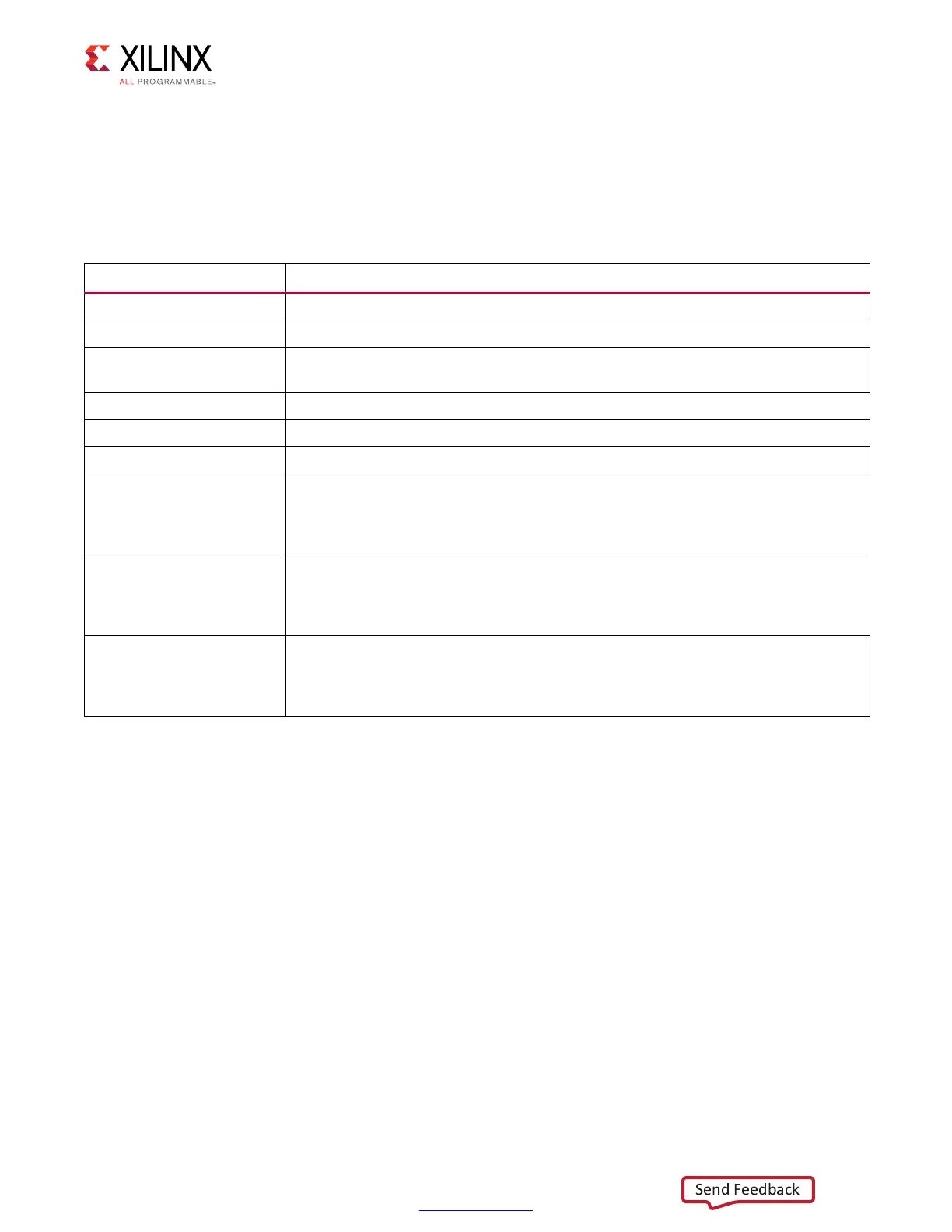
Table 1-75: Debug Signals of Interest for DQSFOUND Calibration
Signal Name Description
dbg_pi_dqsfound_start Signifies the start of the DQSFOUND stage of calibration.
dbg_pi_dqsfound_done Signifies successful completion of the DQSFOUND stage of calibration.
dbg_pi_dqsfound_err
Signifies the DQSFOUND stage of calibration exhibited errors and did not
complete.
dbg_rd_data_offset_0 Read Data Offset found during calibration.
dbg_calib_rd_data_offset_1 Read Data Offset found during calibration.
dbg_calib_rd_data_offset_2 Read Data Offset found during calibration.
dbg_data_offset
Data Offset used during normal operation. Value changes during writes, reads, and
idle. During writes, it is CWL+2+slot#. During non-data commands, it is 0. During
reads, it should match what was found during DQSFOUND calibration
(rd_data_offset_ranks).
dbg_data_offset_1
Data Offset used during normal operation. Value changes during writes, reads, and
idle. During writes, it is CWL+2+slot#. During non-data commands, it is 0. During
reads, it should match what was found during DQSFOUND calibration
(rd_data_offset_ranks).
dbg_data_offset_2
Data Offset used during normal operation. Value changes during writes, reads, and
idle. During writes, it is CWL+2+slot#. During non-data commands, it is 0. During
reads, it should match what was found during DQSFOUND calibration
(rd_data_offset_ranks).
 Loading...


