Zynq-7000 AP SoC and 7 Series FPGAs MIS v4.1 453
UG586 November 30, 2016
www.xilinx.com
Chapter 3: RLDRAM II and RLDRAM 3 Memory Interface Solutions
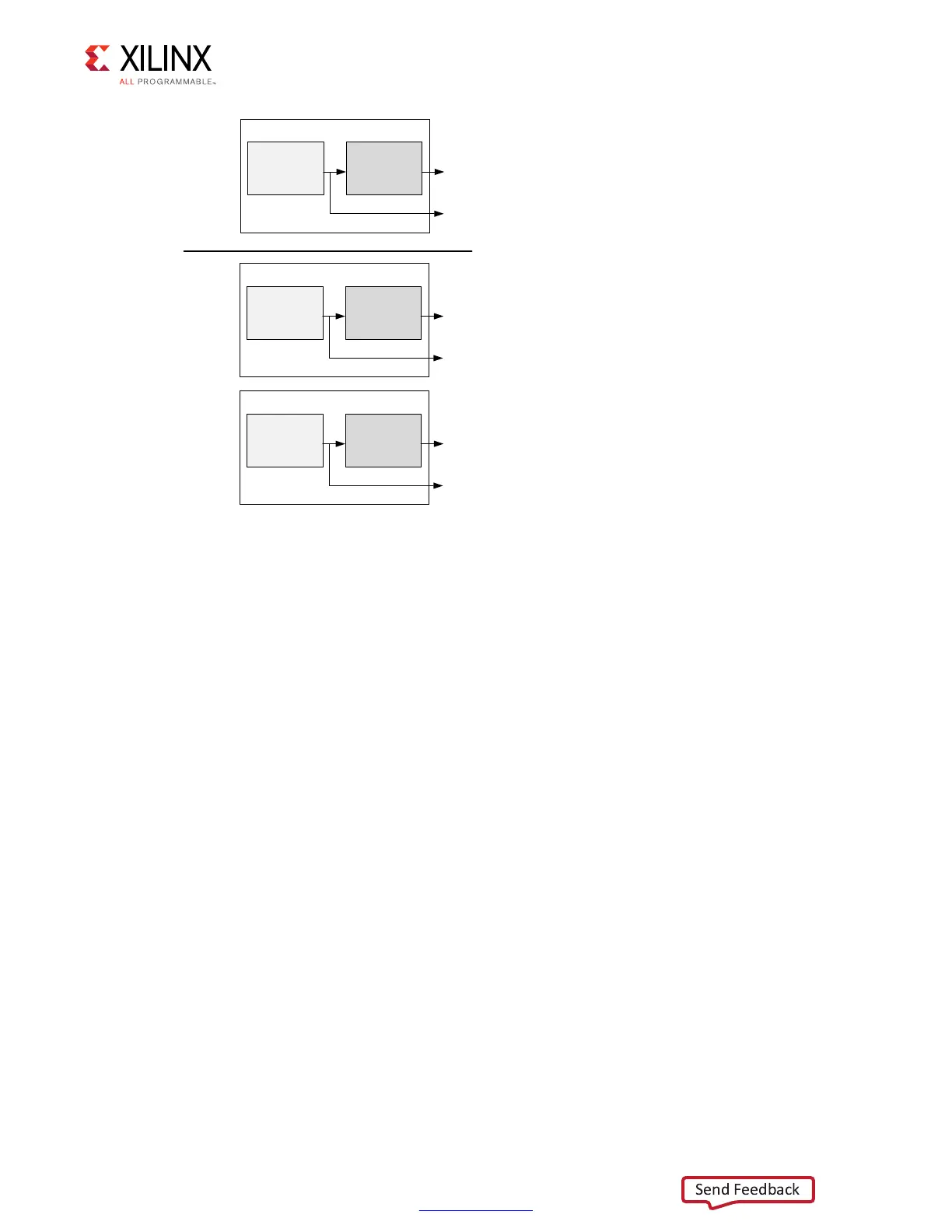
The first stage of RLDRAM II write calibration is to calibrate DK clock with respect to DQ in
the same byte lane. The write clock DK is adjusted in relation to the DQ to find the data
valid window and center in that window as shown in Figure 3-55.
X-Ref Target - Figure 3-54
Figure 3-54: RLDRAM II Write Calibration
A/C Bank
(with CK)
DK
DQ
DQ
Step 1: Calibrate byte lanes with DK
(DK moved, stage 3)
Step 2: Calibrate between DK and CK
(DK/DQ moved, stage 2)
Step 3: Calibrate DQ with the DK in another byte lane
(DQ moved, stage 2)
Data Bank
CK
Stage 2 Stage 3
PHASER_OUT
Stage 2 Stage 3
PHASER_OUT
Stage 2 Stage 3
PHASER_OUT
 Loading...


