Zynq-7000 AP SoC and 7 Series FPGAs MIS v4.1 156
UG586 November 30, 2016
www.xilinx.com
Chapter 1: DDR3 and DDR2 SDRAM Memory Interface Solution
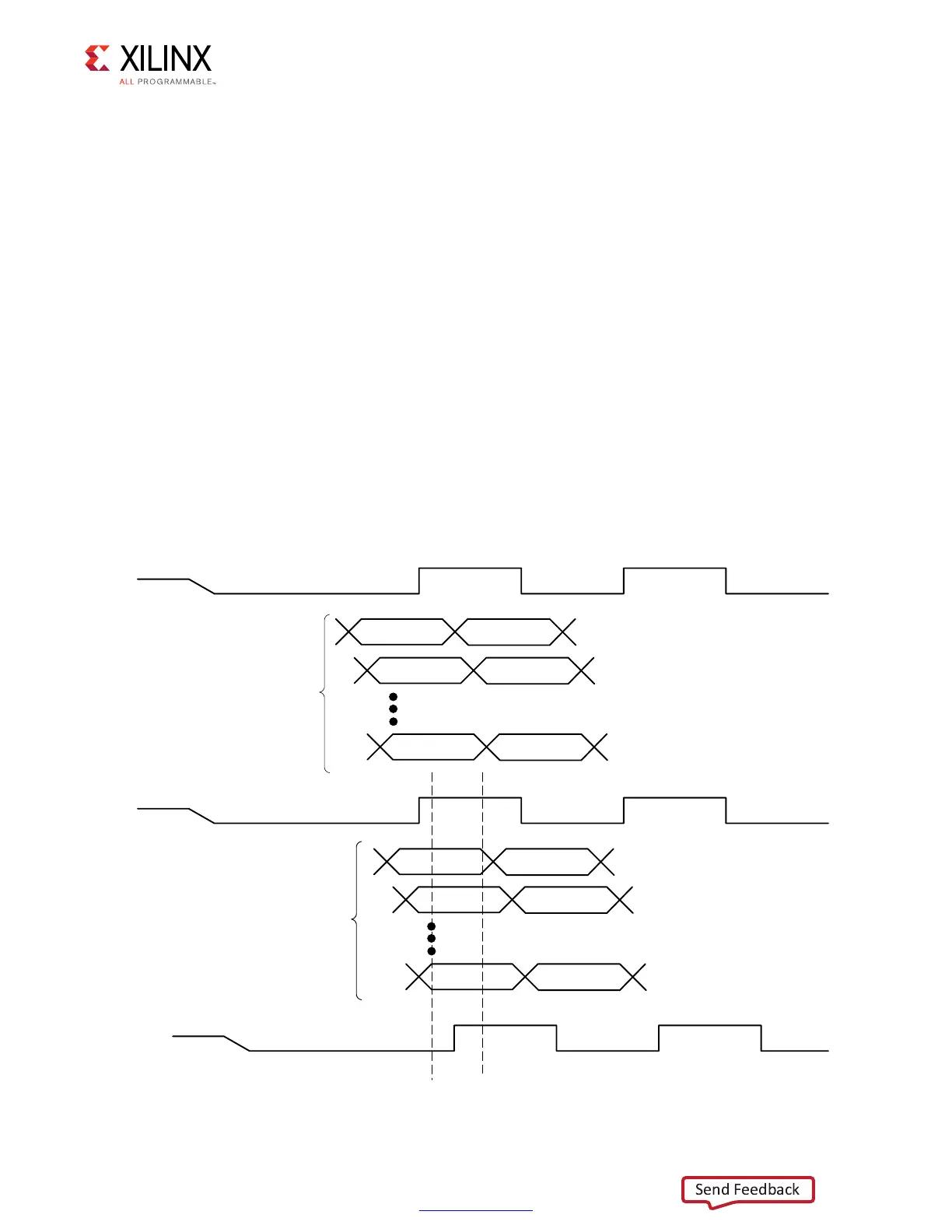
The first two scenarios would result in the left data window edge being detected with a tap
count less than 1/2 the bit time and the second window edge might or might not be
detected, depending on the frequency and the width of the noise region. The third scenario
results in the right window edge being detected with a tap count close to a bit time. When
both edges are detected, the final DQS tap value is computed as:
first_edge_taps + (second_edge_taps – first_edge_taps)/2.
When only one edge is detected and the tap value of the detected edge is less than 1/2 of
a bit time, the final DQS tap value is computed as:
(first_edge_taps + (63 – first_edge_taps)/2)
When only one edge is detected and the tap value of the detected edge is almost a bit time,
the final DQS tap value is computed as:
(63 – (63 – first_edge_taps/2))
Figure 1-71 shows the timing diagram for DQS center alignment in the data valid window.
X-Ref Target - Figure 1-71
Figure 1-71: Read Leveling Stage 1 Timing Diagram
)NITIAL$13
)NITIAL$1"ITS
$1"ITS$ELAYEDUSING
)$%,!94APS
8
$13AT,EFT7INDOW%DGE
$13#ENTEREDIN6ALID
7INDOW
 Loading...


