Zynq-7000 AP SoC and 7 Series FPGAs MIS v4.1 173
UG586 November 30, 2016
www.xilinx.com
Chapter 1: DDR3 and DDR2 SDRAM Memory Interface Solution
In Figure 1-86, requests 1 and 2 are accepted normally. The first time request 3 is presented,
accept is driven Low, and the request is not accepted. The user design retries request 3,
which is accepted on the next attempt. Request 4 is subsequently accepted on the first
attempt.
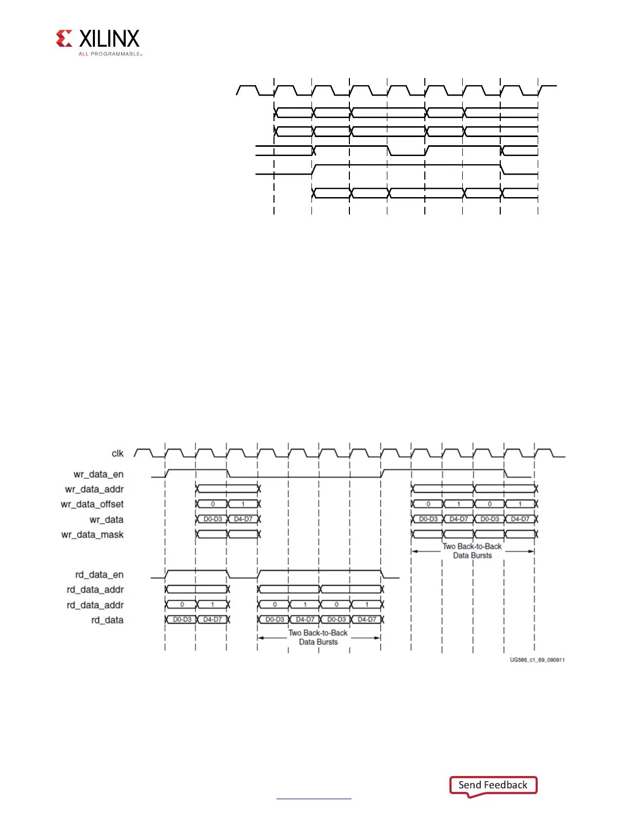
The data_buf_addr bus must be supplied with requests. This bus is an address pointer into
a buffer that exists in the user design. It tells the core where to locate data when processing
write commands and where to place data when processing read commands. When the core
processes a command, the core echoes data_buf_addr back to the user design by
wr_data_addr for write commands and rd_data_addr for read commands. This
behavior is shown in Figure 1-87. Write data must be supplied in the same clock cycle that
wr_data_en is asserted.
X-Ref Target - Figure 1-86
Figure 1-86: Native Interface Flow Control
CLK
RANKBANKROWCOLUMN
CMDHI?PRIORITY
ACCEPT
USE?ADDR
DATA?BUF?ADDR
5'?C??
X-Ref Target - Figure 1-87
Figure 1-87: Command Processing