Zynq-7000 AP SoC and 7 Series FPGAs MIS v4.1 323
UG586 November 30, 2016
www.xilinx.com
Chapter 2: QDR II+ Memory Interface Solution
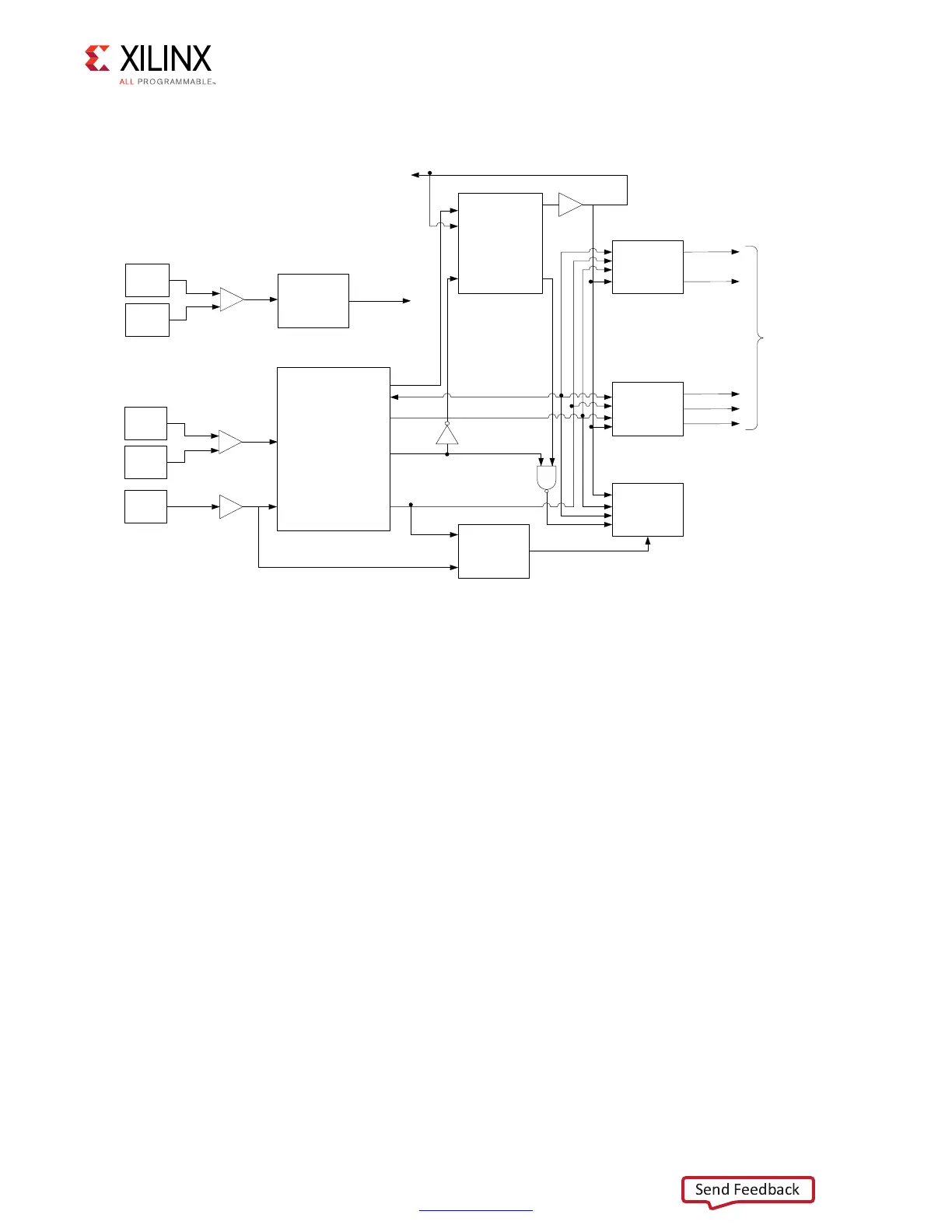
Figure 2-41 shows the clocking architecture.
The default setting for the PLL multiply (M) and divide (D) values is for the system clock
input frequency to be equal to the memory clock frequency. This 1:1 ratio is not required.
The PLL input divider (D) can be any value listed in the 7 Series FPGAs Clocking Resources
User Guide (UG472) [Ref 10] as long as the PLLE2 operating conditions are met and the
other constraints listed here are observed.
The PLL multiply (M) value must be between 1 and 16 inclusive. The PLL VCO frequency
range must be kept in the range specified in the silicon data sheet. The sync_pulse must
be 1/16 of the mem_refclk frequency and must have a duty cycle of 1/16 or 6.25%. For
information on physical placement of the PLL and the System Clock CCIO input, see Design
Guidelines, page 342.
The internal FPGA logic clock generated by the PLL is clocked by a global clocking resource
at half the frequency of the QDR II+ memory frequency.
A 200 MHz IDELAY reference clock must be supplied to the IDELAYCTRL module. The
IDELAYCTRL module continuously calibrates the IDELAY elements in the I/O region to
account for varying environmental conditions. The IP core assumes an external clock signal
is driving the IDELAYCTRL module. If a PLL clock drives the IDELAYCTRL input clock, the PLL
lock signal needs to be incorporated in the rst_tmp_idelay signal inside the
IODELAY_CTRL module. This ensures that the clock is stable before being used.
X-Ref Target - Figure 2-41
Figure 2-41: Clocking Architecture
CLKREF
N
CLKREF
P
Phaser_IN
Phaser_OUT
PHY Control
0+],'(/$<
5HIHUHQFH&ORFN
IDELAYCTRL
LGHOD\FWUOBUG\
MMCM
&/.,1
&/.)%287
/2&.('
&/.)%,1
567
PHASER_REF
&/.,1
567
PLL
&/.,1
&/.287
&/.287567
&/.287
&/.287
/2&.('
SYSCKN
SYSCKP
6\VWHP&ORFN,QSXW3DLU
SYSRST
,%8)*'6
,%8)
UHIBGOOBORFN
2&/.
2&/.',9
2&/.B'(/$<('
,&/.
,&/.',9
,QWHUQDO)3*$/RJLF&ORFN
IUHTBUHIFON
3+<B&ON
%8)*
V\QFBSXOVH
PHPBUHIFON
SOOBORFN
,6(5'(626(5'(6
&RQQHFWLYLW\
;
,%8)*'6
 Loading...


