Zynq-7000 AP SoC and 7 Series FPGAs MIS v4.1 456
UG586 November 30, 2016
www.xilinx.com
Chapter 3: RLDRAM II and RLDRAM 3 Memory Interface Solutions
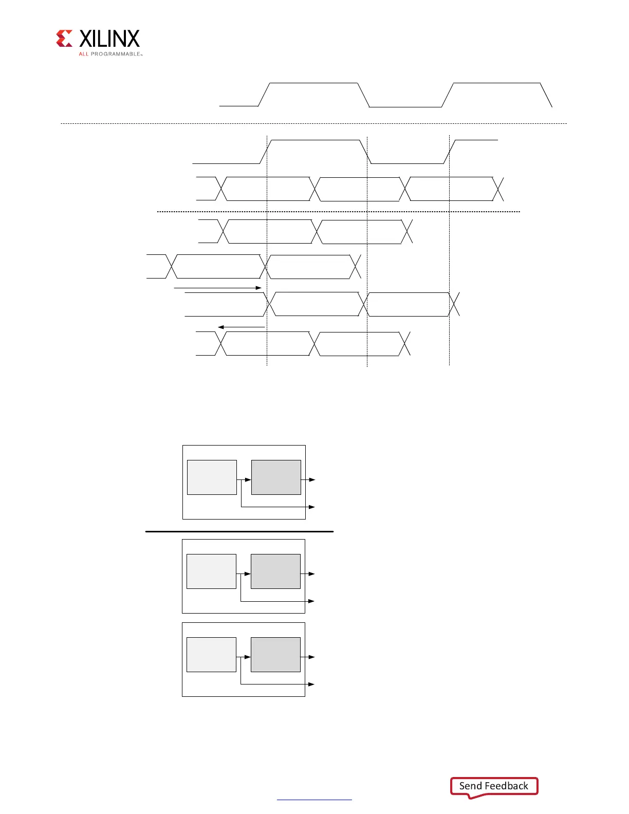
Figure 3-58 shows the RLDRAM 3 pinout with two data byte lanes and the overview for the
steps taken for write calibration.
X-Ref Target - Figure 3-57
Figure 3-57: RLDRAM II Write Calibration (Stage 3, DK-to-DQ2)
Byte lane
without a
DK
Rise
DQ
Fall
Rise
DQ
Fall
Starting
point, 32
taps
Rise
DQ
Fall
Start the
sweep at
0 taps
Sweep until window
edge found or end
of taps
(1)
(2)
(3)
Rise
DQ
Fall
Final
Setting
(4)
Data Shift
Data Shift
Fall
A/C Bank
CK
Rise
DQ
Fall
Rise
DK
Byte lane
with a DK
X-Ref Target - Figure 3-58
Figure 3-58: RLDRAM 3 Write Calibration
A/C Bank
(with CK)
DQ
DQ
Step 1: Calibrate DQ with the DK in another
byte lane (DQ moved, stage 2)
Data Bank
CK
Stage 2 Stage 3
PHASER_OUT
Stage 2 Stage 3
PHASER_OUT
Stage 2 Stage 3
PHASER_OUT
DK
 Loading...


