CHAPTER 2 NEW FUNCTIONS
2-77
COPYRIGHT
©
2001 CANON INC. 2000 2000 2000 2000 CANON iR8500/7200 REV.1 AUG. 2001
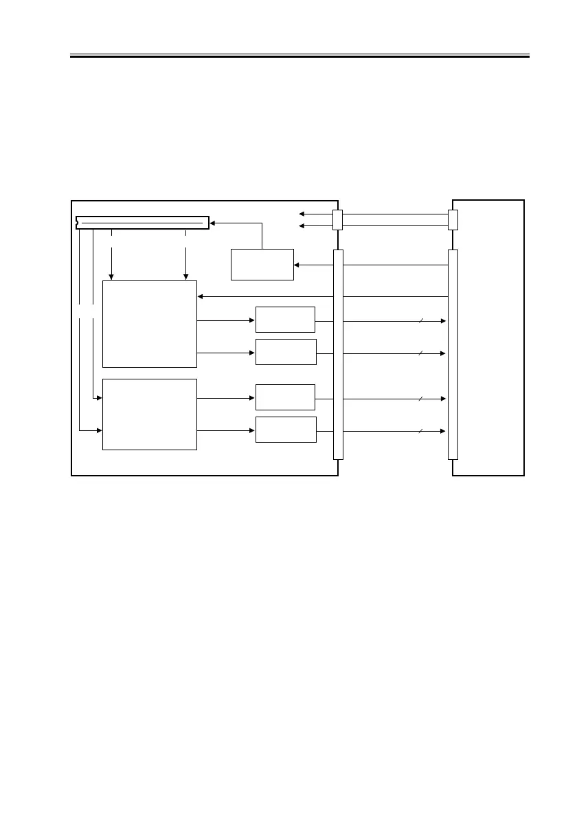
4.5 Analog Image Processing
Analog image processing is performed on the CCD/AP PCB, and consists of the follow-
ing main items:
• Driving the CCD
• Executing gain correction for the CCD output, executing offset correction
• Executing A/D conversion for the CCD output
[1] First half even-number pixel analog image signal
[2] First half odd-number pixel analog image signal
[3] Last half even-number pixel analog image signal
[4] Last half odd-number pixel analog image signal
[5] First half even-number pixel analog image signal
[6] First half odd-number pixel digital image signal
[7] Last half even-number pixel digital image signal
[8] Last half odd-number pixel digital image signal
F02-405-01
CCD
Analog signal
processing block
• Gain correction
• Offset correction
A/D
conversion
A/D
conversion
Analog image
signal
CCD/AP PCB
CCD drive
control
Reader
controller
PCB
10bit
J1502
J1501
J1107
J1102
10
10
10
CCD control signal
A12V
A5V
Gain/offset
correction data
[2] [1]
[1]
[2]
Analog signal
processing block
• Gain correction
• Offset correction
A/D
conversion
A/D
conversion
[3]
[4]
[5]
[6]
[7]
[8]
[4] [3]
 Loading...