CHAPTER 2 NEW FUNCTIONS
2-87
COPYRIGHT
©
2001 CANON INC. 2000 2000 2000 2000 CANON iR8500/7200 REV.1 AUG. 2001
5.2 Analog Image Processing
5.2.1 Outline
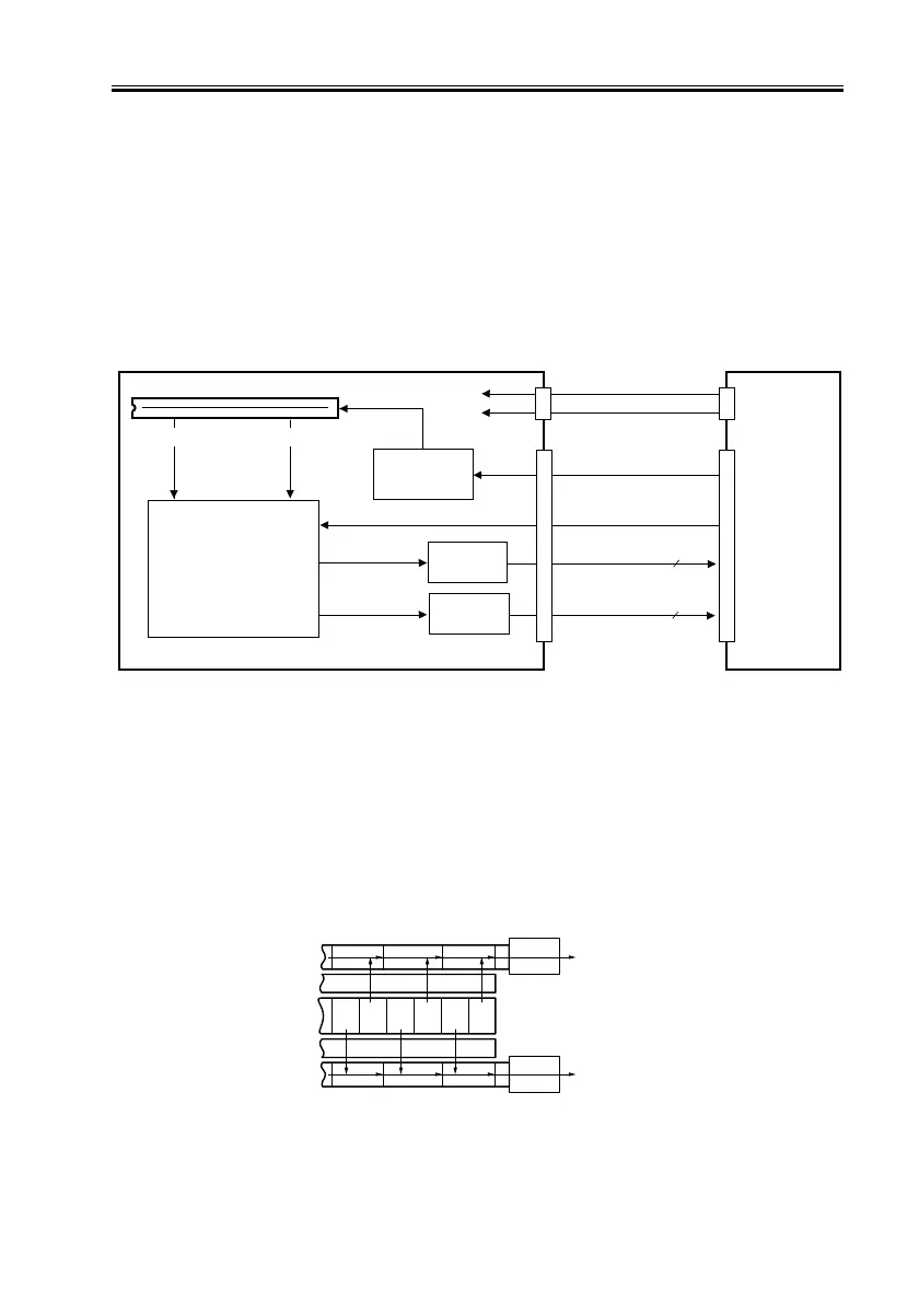
Analog image processing is performed by the CCD/AP PCB, which has the following
major functions:
[1] Drives the CCD.
[2] Corrects the gain in the CCD output, corrects offset.
[3] Performs A/D conversion of CCD output.
F02-502-01
5.2.2 Driving the CCD
The machine’s CCD sensor is a single-line linear image sensor, and is composed of 7450
pixel photo cells.
The signals subjected to phtoconversion in the light-receiving segment are sent out in two
types of analog signals: even-number (EVEN) pixels and odd-number (ODD) pixels.
F02-502-02 CCD Block Diagram
CCD
Analog signal
processing unit
· Gain correction
· Offset correction
A/D
conversion
A/D
conversion
Analog image
signal
Digital image signal
CCD/AP PCB
CCD drive
control
Reader
controller
PCB
8
J6002
J6001
J5003
J5002
Even-number pixels
Odd-number pixels
Even-number
pixels
Odd-number
pixels
Digital image signal
8
CCD control signal
A12V
A5V
Gain/offset
correction data
Shift register
Light receiving
segment
(photodiode)
Shift register
Output buffer
Output buffer
Gate
Gate
123456
Odd-number pixel data
Even-number pixel data
 Loading...